In today’s world of ever-shrinking electronics and increasingly complex functionalities, High-Density Interconnect (HDI) PCBs have become indispensable. These sophisticated boards pack more circuitry into a smaller space compared to traditional PCBs, enabling the miniaturization of devices while boosting performance. From smartphones and wearables to advanced medical devices and aerospace applications, HDI PCBs are revolutionizing the electronics landscape.
What Defines an HDI PCB?
While there isn’t a single, universally agreed-upon definition, HDI PCBs generally exhibit some or all of the following characteristics:
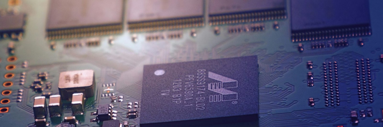
- Microvias: These are tiny vias (interconnects between layers) with a diameter of ≤150µm, often created using laser drilling. They allow for denser routing and improved signal integrity.
- Blind and Buried Vias: Unlike through-hole vias that pass through the entire board, blind vias connect an outer layer to one or more inner layers, while buried vias connect only inner layers. These save space on the surface and increase routing density.
- Fine Lines and Spaces: HDI PCBs utilize narrower traces and spaces (typically ≤100µm) than conventional PCBs, allowing for more circuits in the same area.
- High Density of Interconnects: The overall number of connections per unit area is significantly higher in HDI PCBs due to the use of microvias and fine lines.
- Sequential Lamination: More complex HDI boards might involve multiple lamination cycles, adding layers incrementally to achieve the desired interconnect density.
Benefits of HDI PCBs:
The adoption of HDI technology offers a multitude of advantages:
- Miniaturization: HDI PCBs enable the creation of smaller and lighter electronic devices, crucial for applications like wearables and portable electronics.
- Increased Functionality: By packing more circuitry into a smaller space, HDI PCBs allow for more complex and feature-rich devices.
- Improved Signal Integrity: Shorter trace lengths and the use of microvias minimize signal distortion and improve high-speed performance.
- Enhanced Thermal Performance: HDI structures can improve heat dissipation, leading to more reliable operation.
- Reduced Layer Count: In some cases, HDI techniques can allow for a reduction in the overall layer count compared to a traditional PCB achieving the same functionality, leading to cost savings.
Manufacturing Challenges:
Manufacturing HDI PCBs presents several challenges:
- Precise Microvia Formation: Laser drilling of microvias requires highly accurate equipment and process control.
- Fine Line Etching: Creating fine lines and spaces demands precise etching techniques to avoid defects.
- Sequential Lamination Complexity: Multiple lamination cycles add complexity to the manufacturing process and require careful alignment.
- Material Selection: HDI PCBs often require specialized materials with specific electrical and thermal properties.
- Testing and Inspection: Testing and inspecting HDI boards can be more challenging due to the high density of interconnects.
Applications of HDI PCBs:
HDI PCBs find applications in a wide range of industries:
- Consumer Electronics: Smartphones, tablets, laptops, wearables, and other portable devices.
- Medical Devices: Implantable devices, diagnostic equipment, and other advanced medical electronics.
- Automotive: Advanced driver-assistance systems (ADAS), infotainment systems, and other automotive electronics.
- Aerospace and Defense: Avionics, communication systems, and other high-reliability applications.
- Telecommunications: Networking equipment, routers, and other communication infrastructure.
The Future of HDI PCBs:
As electronic devices continue to shrink and become more complex, HDI technology will play an even greater role. Ongoing advancements in materials, manufacturing processes, and design techniques are pushing the boundaries of HDI PCBs, enabling even higher densities and improved performance. We can expect to see further innovations in microvia technology, finer line widths, and new substrate materials, paving the way for the next generation of electronic devices. The continued development of HDI PCBs is essential for driving innovation and shaping the future of technology.